


Description:
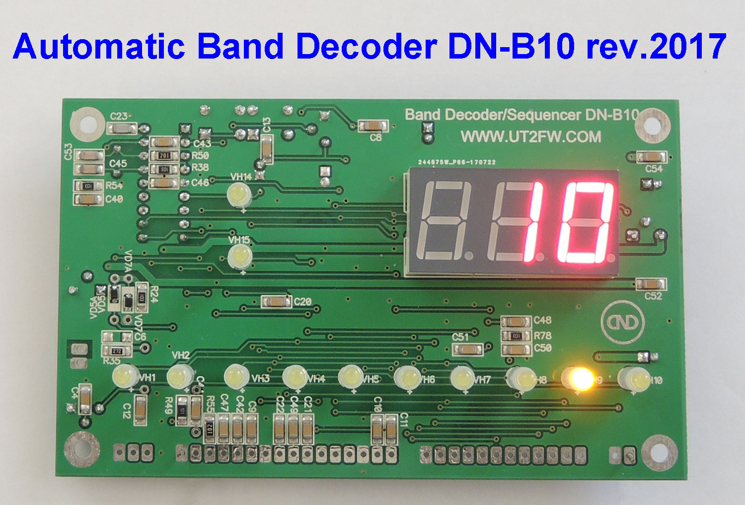
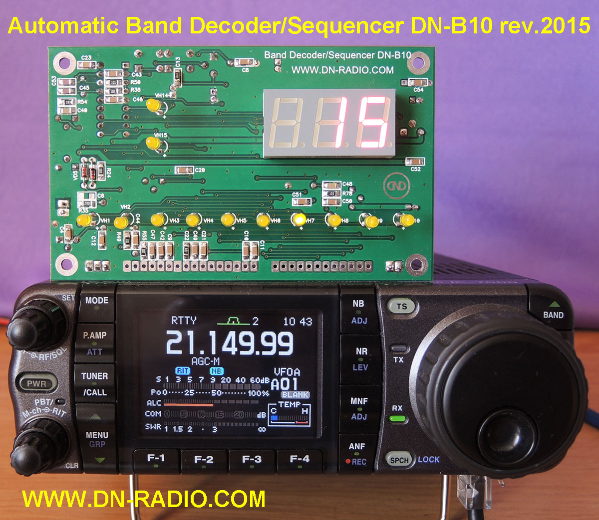
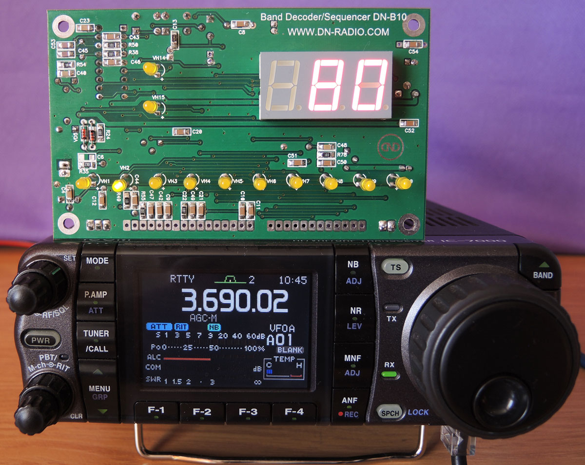
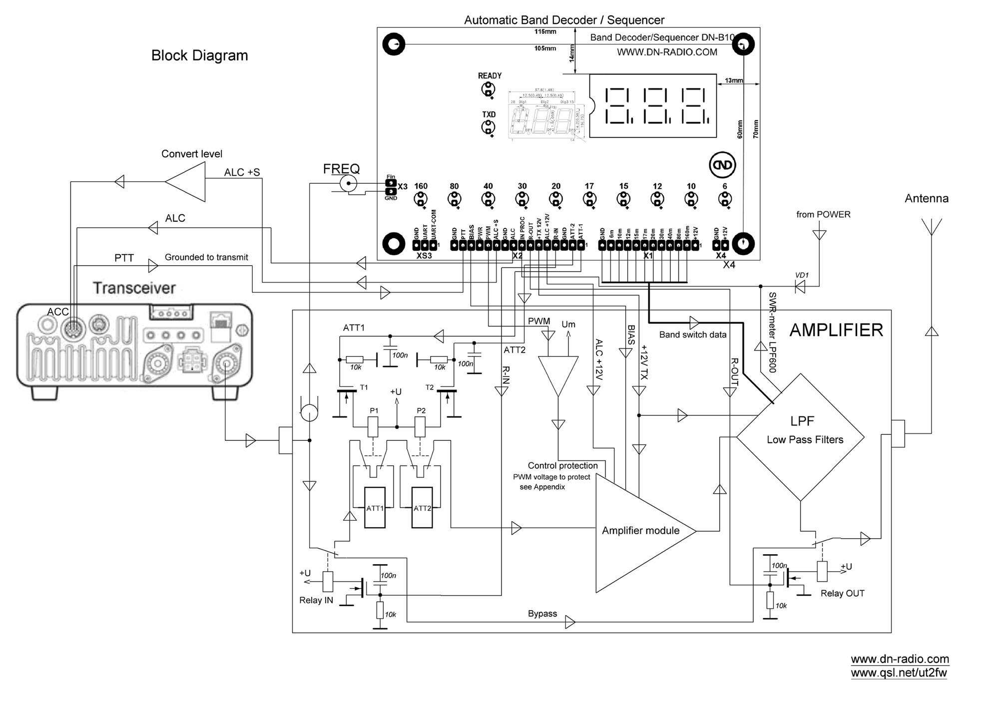
Automatic Band Decoder/Sequencer DN-B10
The main objective in the manufacture of high-power amplifier is ensuring high reliability. If the protection of the amplifier had not carefully designed, an accident can happen at any inopportune moment.
All switchings in amplifier should be connected to each other and occur by a single algorithm.
The functions execution algorithm required to consider both the characteristics of building amplifier, and the specifics of HAM Radio applications.
An important requirement for HAM engineering is low cost.
The Band Decoder/Sequencer DN-B10 is based on these requirements.
The device is designed for automatic control of switching-mode RX-TX, LPF filters, ATT, BIAS and amplifier protection.
It can be used to automatically select any devices in accordance with the frequency of the signal applied to the Band Decoder. For example, to switch antennas, filters, amplifiers.
The principle of operation of the Band Decoder based on the measuring the frequency of the signal from the transmitter (Automatic band change based on TX frequency).
It is sufficiently high frequency voltage from ~5V for stable operation, which corresponds to the power of 0.5 W at impedance of 50Ohm.
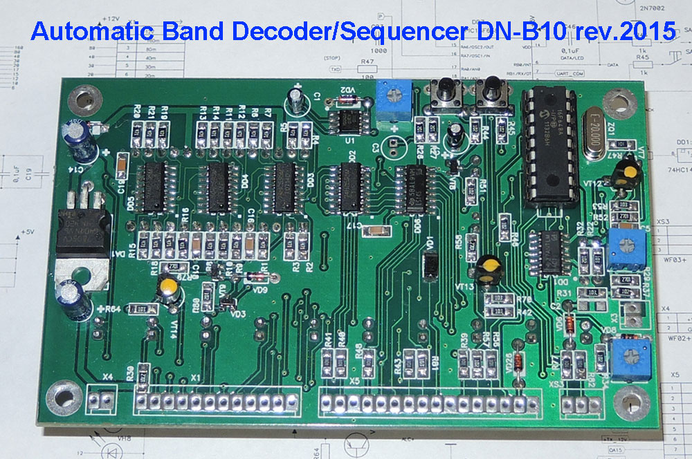
The control of the Band Decoder performs the microprocessor PIC16F648A. The cymometer of the microprocessor determines the frequency of the input signal and sets the appropriate range. The minimum tuning step of frequency is 10kHz. Border ranges are distributed as follows:
1.0 – 2.5MHz – 160m;
2.51 – 4.0MHz – 80m;
4.01 – 8.0MHz – 40m;
8.01 – 11.0MHz – 30m;
11.01 – 16.0MHz – 20m;
16.01 – 20.0MHz – 17m;
20.01 – 23.0MHz – 15m;
23.01 – 26.0MHz – 12m;
26.01 – 31.0MHz – 10m;
31.01 – 55MHz – 6m;
The Sequencer controls the operation mode switching RX-TX amplifier. For safe switching is observed a certain sequence of control signals. The algorithm was written in the program of the microprocessor.
The order of the amplifier from the RX-mode to the TX-mode is as follows:
1.The Band Decoder turns on corresponding range filter in the amplifier.
2.It is measured the input power. If the input power exceeds the power recorded in the memory of the microprocessor – it prohibits the next step and stops the work. The indicators of the range are blinking in this case.
If the power does not exceed the power recorded in the memory of the microprocessor – it allows the next step – turning on the Sequencer.
The Sequencer is turning on from the PTT signal from the transceiver.
3.ALC reduces the power of the transceiver to 0W at 50mS.
4.During 50mS while ALC is turned on, the antenna is connected to the output of the amplifier. The delay of the antenna relay is 40mS.
5.The amplifier input is connected to the transceiver. The delay of the relay is 10mS.
6.The voltage BIAS is served .
7.ALC increases the power of the transceiver to the nominal.
8.When the transceiver is returned to RX-mode the Sequencer is turning off and the amplifier is switching to the RX-mode.
The Band Decoder can operate autonomously. It is enough only to submit the frequency on it.
Screenshots of the waveforms of control signals:
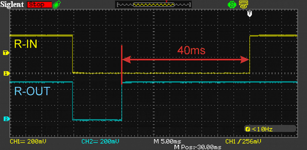
R-IN <–> R-OUT
R-IN <-> BIAS

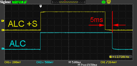
ALC+S <-> ALC
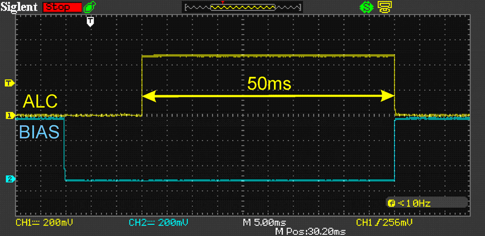
ALC <-> BIAS
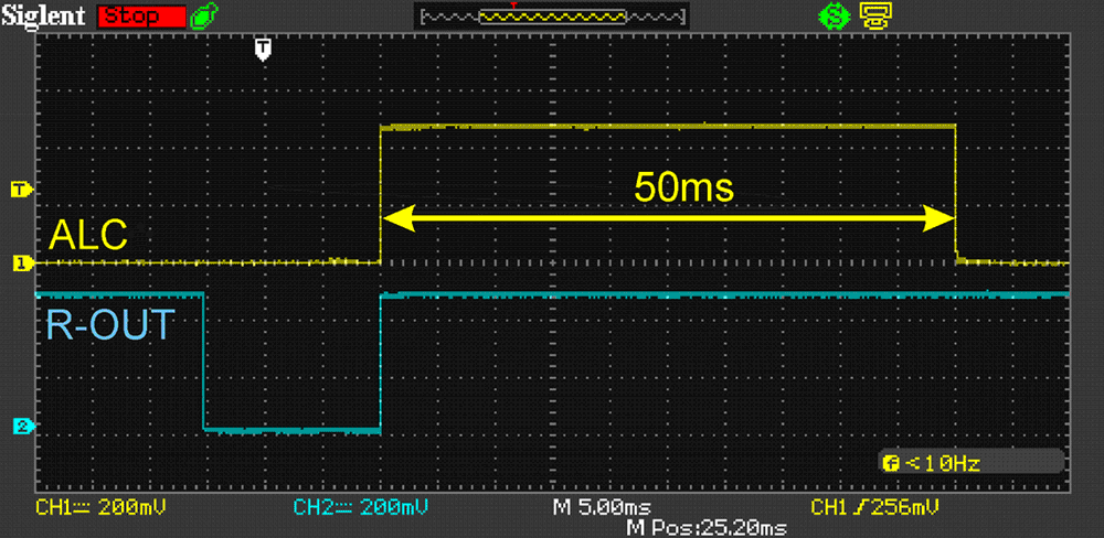
ALC <-> R-OUT
Additional features of Band Decoder/Sequencer.
To obtain the same power range between the transceiver and the amplifier use the attenuator. The Band Decoder/Sequencer can control two attenuators. You can choose of the four state attenuators at any range:
1.Both ATT off.
2.Turns on ATT No. 1.
3.Turns on ATT No. 2.
4.Turn on both ATT.
State of attenuators is selected on the stage of programming the microprocessor.
The original program of turn on used next an algorithm:
160m, 80m, 40m, 30m – ATT1 on, ATT2 off.
20m, 17m, 15m – ATT2 on, ATT1 off.
12m, 10m, 6m – ATT2, ATT1 off.
For control the protections of the amplifier can be applied the comparator, for example, to overload protection the input of the amplifier. The reference voltage for comparator may vary depending on the range. For the operation of the comparator DN-B10 forms separately for each voltage range PWM.
Two buttons "more-less" select the desired level of voltage and store it to the memory of the microprocessor. Press the button and hold until the voltage reaches the desired value. The indicators will indicate the voltage level in the range of 1-255. The actual voltage at pin PWM will be from 0V to +5V. The values are saved when you turn off the voltage of the Band Decoder/Sequencer.

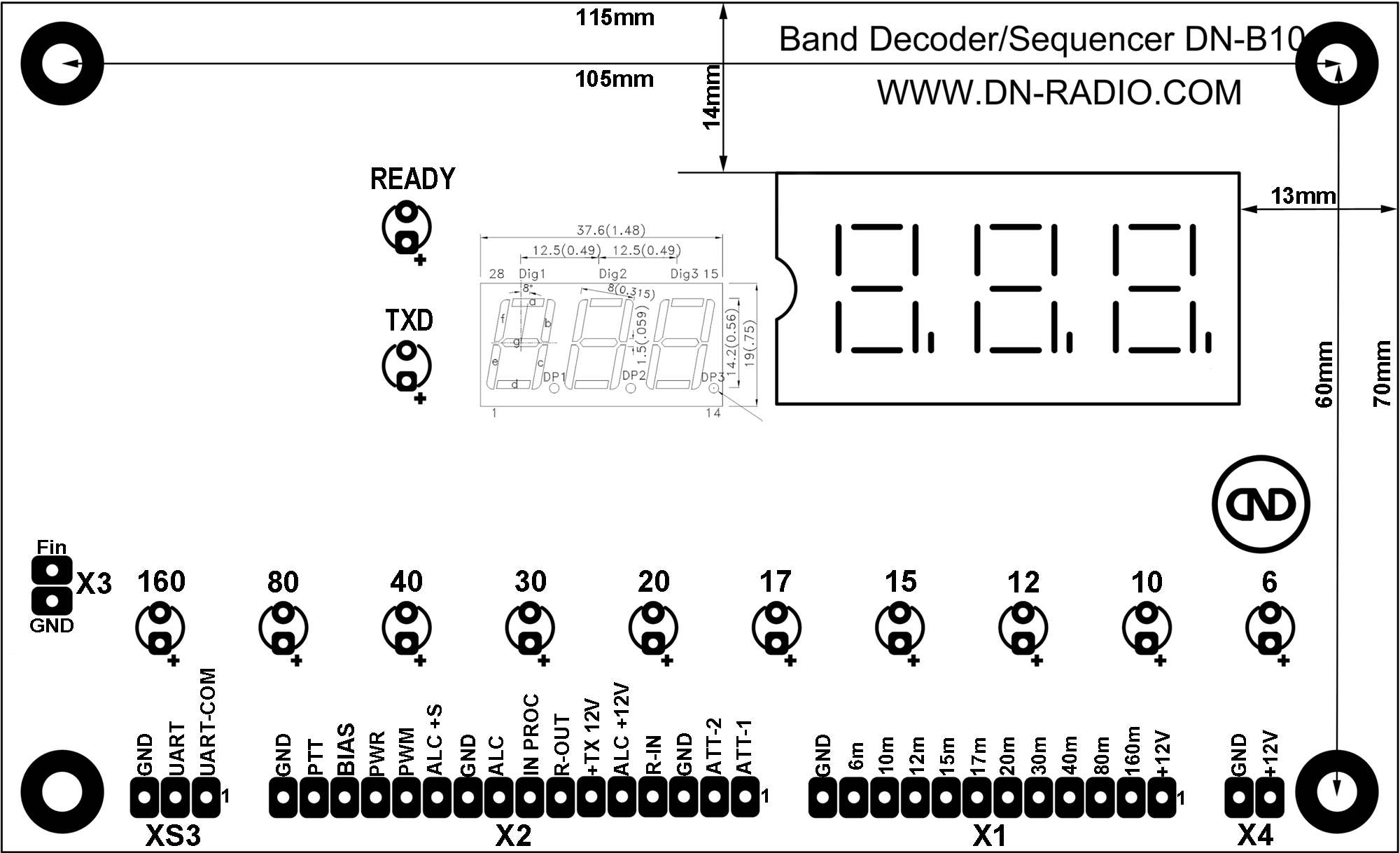
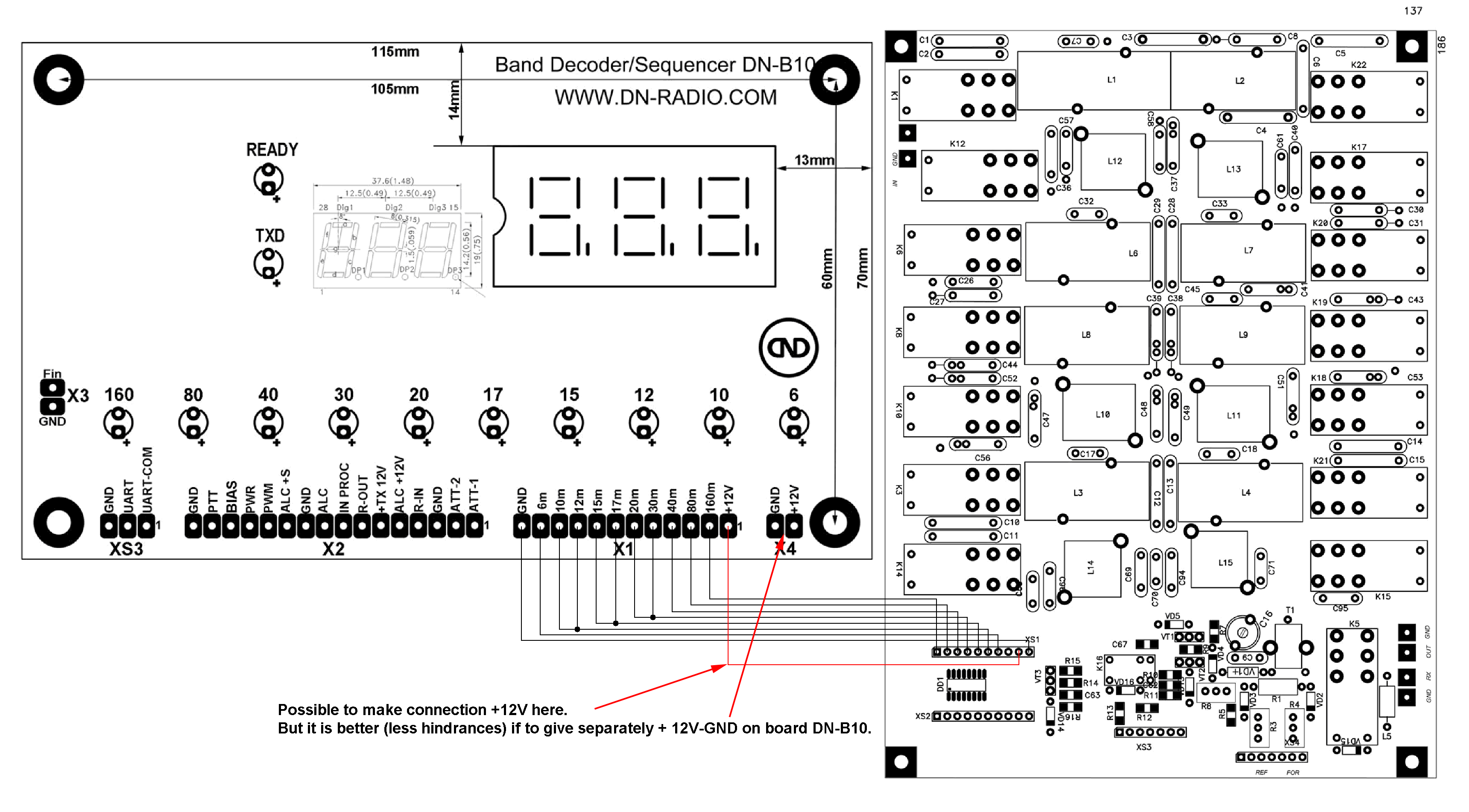
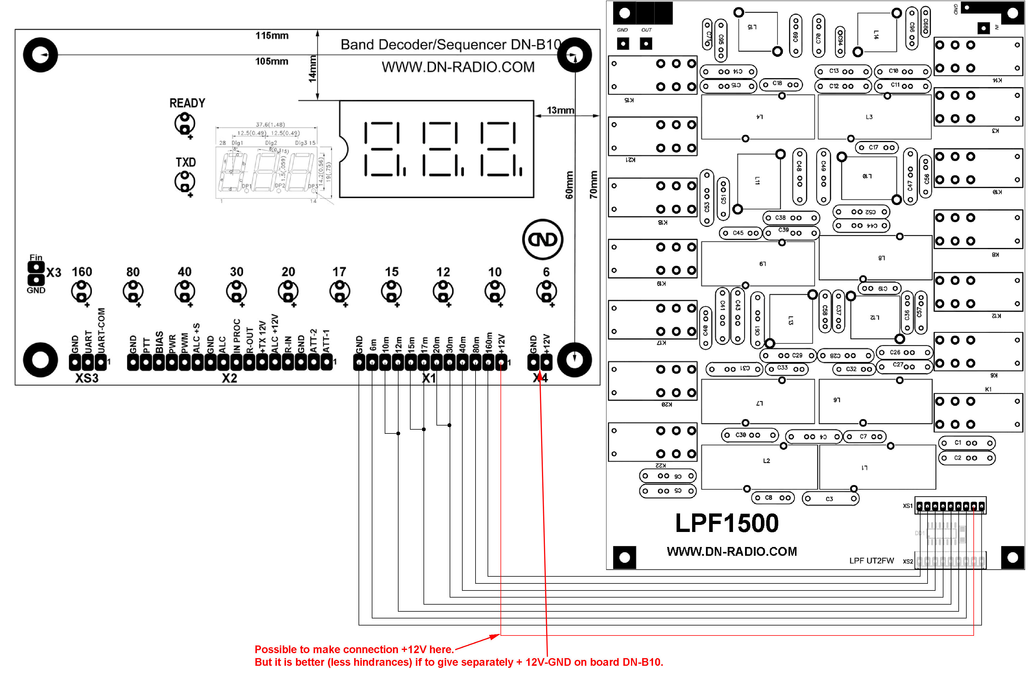
The pinout of connectors.
X1 Pinout
|
PIN |
SIGNAL |
DESCRIPTION |
|
1 |
+12V |
Output +12V. Connected in parallel to a contact +12V X4. |
|
2 |
160m |
Open collector 74LS145. Current up to 80mA, voltage up to 15V. |
|
3 |
80m |
Open collector 74LS145. Current up to 80mA, voltage up to 15V. |
|
4 |
40m |
Open collector 74LS145. Current up to 80mA, voltage up to 15V. |
|
5 |
30m |
Open collector 74LS145. Current up to 80mA, voltage up to 15V. |
|
6 |
20m |
Open collector 74LS145. Current up to 80mA, voltage up to 15V. |
|
7 |
17m |
Open collector 74LS145. Current up to 80mA, voltage up to 15V. |
|
8 |
15m |
Open collector 74LS145. Current up to 80mA, voltage up to 15V. |
|
9 |
12m |
Open collector 74LS145. Current up to 80mA, voltage up to 15V. |
|
10 |
10m |
Open collector 74LS145. Current up to 80mA, voltage up to 15V. |
|
11 |
6m |
Open collector 74LS145. Current up to 80mA, voltage up to 15V. |
|
12 |
GND |
Ground. |
X2 Pinout
|
PIN |
SIGNAL |
DESCRIPTION |
|
1 |
ATT1 |
Control of the ATT1 relay. TTL output +5V up to 10mA. |
|
2 |
ATT2 |
Control of the ATT2 relay. TTL output +5V up to 10mA. |
|
3 |
GND |
Ground. |
|
4 |
R-IN |
Control of the IN-relay. TTL output +5V up to 10mA. |
|
5 |
ALC+12V |
Control transmission power of the transceiver. Output +12V to 100mA. |
|
6 |
+TX 12V |
Voltage +12V TX. Output +12V to 100mA. |
|
7 |
R-OUT |
Control of the OUT-relay. TTL output +5V up to 10mA. |
|
8 |
IN PROC |
Input. External control of ALC+12V and ALC. Apply +5-12V. |
|
9 |
ALC |
Control of ALC of the transceiver. Adjustable output from 0V to -9V, to 10mA. |
|
10 |
GND |
Ground. |
|
11 |
ALC+ |
Control of ALC of the transceiver. TTL output +5V up to 10mA. |
|
12 |
PWM |
Control of the protection, voltage from 0V to + 5V. The load current is less than 0,5mA. Rl > 10k. |
|
13 |
PWR |
Input. Disables the control of the LPF relay. Apply +5V. |
|
14 |
BIAS |
The bias voltage for the transistors of the amplifier. Output +12V to 100mA. |
|
15 |
PTT |
PTT input. Shorted to ground for translation in the TX-mode. |
|
16 |
GND |
Ground. |
X3 Pinout
|
PIN |
SIGNAL |
DESCRIPTION |
|
1 |
Fin |
Input for measurement of frequency. The minimum level of ~5V. |
|
2 |
GND |
Ground. Power supply return. Chassis ground. |
X4 Pinout
|
PIN |
SIGNAL |
DESCRIPTION |
|
1 |
+12V |
The supply voltage from +12VDC to +14VDC. The current consumption 80mA. |
|
2 |
GND |
Ground. Power supply return. Chassis ground. |
Application of the Band Decoder/Sequencer.
For the power of the Band Decoder/Sequencer used sufficiently stabilized voltage 5V, current up to 80mA. But for the unification of the supply voltage is applied the additional stabilizer DA1 7805. Therefore, the supply voltage may not be stable and range from +12VDC to +14VDC. The higher the voltage than the stronger will be heated 7805. Increasing the voltage will increase the power that is dissipated on DA1. Power is supplied to connector X4.
The limit voltage of the input frequency Fin ~5V to ~70V. The optimum value of the voltage Fin ~15V to ~30V. The sensitivity of the Fin input is adjustable with variable resistor (trimmer) R23. The sensitivity of the Fin input sets on a stable working of the cymometer on all bands. To adjust the sensitivity of the Fin should be at smaller power values. To start the adjustment in position of the rolling contact R23 closer to the output connected with ground. Frequency is served to connector X3.
The sensitivity of the input of the input power meter P is adjusted by a variable resistor (trimmer) R25.
The ALC voltage to control the transceiver is adjusted by a variable resistor (trimmer) R36 in the range from 0V to -9V.
For control of the Low Pass Filters relay is used DD6 74LS145D. The limiting parameters of one key of this chip are the current up to 80mA, the voltage up to 15V. Key – transistor with open collector. The LPF relay must be diode device is activated from the surge reverse current. The outputs the keys of the chip output to the X1 connector.
The measured input power – Pin is the special feature of DN-B10. The power values P are stored in 10 memory cells of the microprocessor separately for each range. When the input power is exceeding the value stored in the memory cell is activated a ban on the next step of the program.
You need to enter the menu to set the voltage level. Before turning on the Band Decoder press and hold the button SA2. Turn on the Band Decoder (apply +12V). The indicators will display tU2. Set the desired voltage level by buttons. Press simultaneously both buttons to save the value. The indicators will display SAF. Now when you turn on each voltage range, the P will be restored to the level saved in the memory of the microprocessor.
As soon as the input power Pin exceeds the level P in the memory cell is activated ban program. Blinking of digits of the range is indicated for the ban. Accordingly, the Sequencer doesn't turn on and the amplifier doesn't go to TX mode.
The ALC+12V, ALC+S, ALC signals will appear and BIAS turns off if the value Pin exceeds the value P when the Sequencer is turned on. Thus the power of the transceiver will decrease and protection system will switch the amplifier to safe mode. The indicators of the range will blink and the operation of the Sequencer will be blocked until switch to the mode RX.
The power level for the measurement is adjusted R25. It is desirable to set this level Pin to measure when the values of P will be close to the maximum value of 10-14. This minimizes the hazardous impact of inductions on the circuit of the power measurement.
The Sequencer control signals are output to the connector X2.
Pin #1. The ATT1 output – TTL +5V, up to 10mA.
Pin #2. The ATT2 output – TTL +5V, up to 10mA.
The Appendix contains the schemes of use ATT1; ATT2.
Pin #3. The ground GND. Connect the negative supply voltage.
Pin #4. The R-IN output – TTL +5V, up to 10mA. The R-IN signal is formed by turn on PTT and the Sequencer. It is controls the input relay of the amplifier. R-IN signal appears after 40mS after R-OUT. The time delay allows to the reliably switch the R-OUT relay.
Apply the powerful R-OUT relay. So it turning on takes more time. The selected time is 40mS. During this time turn on the vast majority of used types of relay. It use of low power R-IN relay. To turn on such relays enough 10mS.
Pin #5. The output ALC+12V – power voltage +12V, up to 100mA. Its function is similar to ALC, but it is another type of output (outgoing) signal. The ALC+12V signal appears only when is the PTT signal and the Sequencer is turned on. The duration of the ALC+12V signal is 50mS since turning on the Sequencer. The Appendix contains the schemes of applying ALC+12V.
Pin #6. The output +TX 12V – the voltage of +12V, up to 100mA. The voltage TX +12V is designed for switching circuits of the amplifier to transmission mode. The voltage appears when you press PTT if the Sequencer is turned on.
Pin #7. The R-OUT output – TTL +5V, up to 10mA. The control of the antenna relay is in the amplifier. It is formed when is the presence of a PTT signal if the Sequencer is (activated) turned on.
Pin #8. The IN-PROC input is an external control of ALC+12V and ALC signals. Apply +5-12V. For example, on the IN-PROC input can be applied a signal from the SWR-meter or the current consumption meter of the amplifier, in case of exceeding of nominal parameters. At the time of apply the signal to IN-PROC input the ALC+12V and ALC signals will appear.
Pin #9. The output ALC is the сontrol of ALC of the transceiver. The voltage can be adjusted by trimmer R36 from 0V to -9V, current up to 10mA. The ALC signal appears only when is the PTT signal and the Sequencer is (activated) turned on. The duration of the ALC signal is 50mS since turning on the Sequencer.
Pin #10. The ground GND. Connect the negative supply voltage.
Pin #11. The output of ALC+S – TTL +5V, up to 10mA. It is the сontrol of ALC of the transceiver. The ALC signal appears only when is the PTT signal and the Sequencer is (activated) turned on. The duration of the ALC+S signal is 45mS since turning on the Sequencer. The ALC+S signal can be used for transceivers with slow ALC.
Pin #12. The PWM output. The voltage of this output can be programmed from 0V to +5V. The load resistance for voltage of PWM should be at least 10k.
You need to enter the menu to set the voltage level. Before turning on the Band Decoder press and hold the button SA1. Turn on the Band Decoder. The indicators will display tU2. Set the desired voltage level by buttons. Press simultaneously both buttons to save the value. The indicators will display SAF. The voltage is stored individually for each range, in ten separate memory cells. Now when turn on the voltage range the PWM will be restored to level stored in memory of the microprocessor. The Appendix contains the schemes of possible application the voltage of PWM in the protection of the amplifier.
Pin #13. The PWR input. It turns off DD6 74LS145D when applying + 5V. You can turn off the control DD6 by activation of the PWR if the amplifier provides additional control of the LPF relay from the switch or the transceiver.
Pin #14. The BIAS output – the voltage of +12V to 100mA. It is the bias voltage for the transistors of the amplifier. The voltage of the BIAS appears after 50mS from R-OUT signal and 10mS from the R-IN signal. Time delays can switch reliably the R-OUT and R-IN relays. Thereby the accident of amplifier is eliminating.
Pin #15. The PTT input. It must be shorted to ground. It is the control of the Sequencer. The +TX 12V; ALC +12V; ALC +S; ALC; R-OUT signals will appear first if not exceeded the threshold of input power P; Through 40mS appears R-IN, then after 10mS appears BIAS and ALC +12V; ALC +S; ALC will turn off. When you turn off PTT the Sequencer is deactivated and all the signals will turn off.
Pin #16. The ground GND. Connect the negative supply voltage.
Appendix
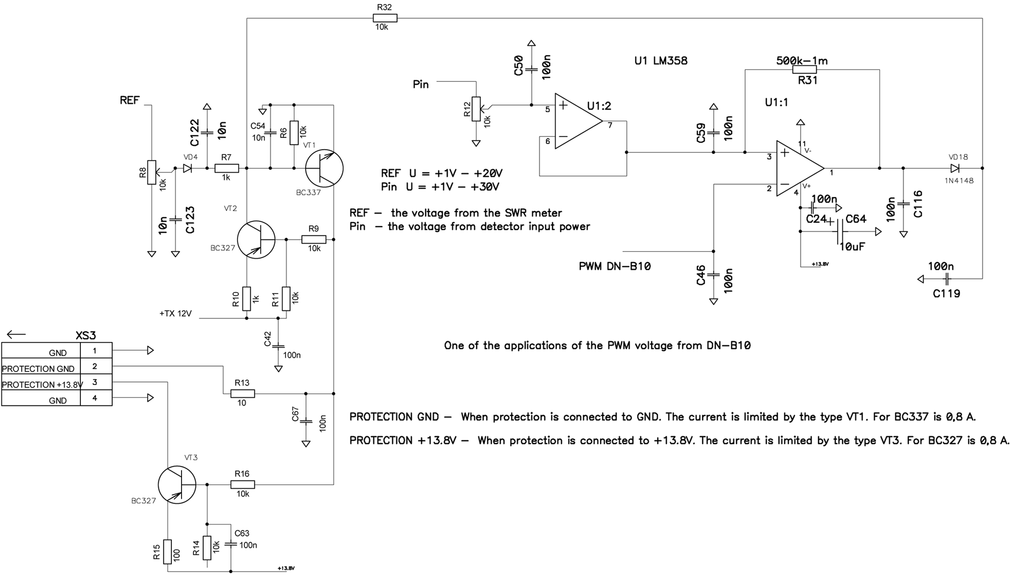
A variant application of PWM voltage to protect the amplifier.
On the example is a circuit protection module LPF600. U1:2 is the follower, U1:1 – the comparator VT1-VT2 commute the voltage, VT2 "locks" the state of the VT1. When removing the voltage TX+12V the circuit returns to its original state.
The REF signal is from the SWR meter. The measured signal labeled as Pin. The output XS3 No. 3 PROTECTION +13.8 V connect to the IN-PROC DN-B10 input. The Pin signal – can be a signal from the current consumption meter of the amplifier.
Very often, the amplifier consumes different current at different ranges. Or the REF signal from the SWR meter, if the antennas have different SWR on different bands. The use of PWM allows you to set the protection individually for each range of the operation.

The link to the YouTube page => https://www.youtube.com/user/UT2FW
Demonstration of work of Band Decoder.